Technology
GCRAM
Important industry growth drivers, such as ML, IoT, Automotive and AR/VR, operate on ever-growing amounts of data that is typically stored off-chip in an external DRAM. Unfortunately, off-chip memory accesses are up-to 1000x more costly in latency and power compared to on-chip data movement. This limits the bandwidth and power efficiency of modern systems. In order to reduce these off-chip data movements, almost all SoCs incorporate large amounts of on-chip embedded memory caches that are typically implemented with SRAM and often constitute over 50% of the silicon area. This memory bottleneck is further aggravated since SRAM scaling has reached its limits and no longer shrinks in advanced CMOS process nodes beyond 5nm.
RAAAM™’s patented GCRAM technology provides up-to 50% area reduction and reduced power consumption by a factor ten ive compared to high-density SRAM by utilizing a unique bitcell solution. This enables increasing the on-chip memory capacity using the same die size to provide a dramatic improvement in system bandwidth and power efficiency through reduction or complete removal of off-chip data movement. Alternatively, reducing the memory footprint can lead to substantial fabrication cost savings through die size reduction.
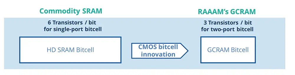
In addition to its area benefits, the GCRAM bit-cell utilizes decoupled write and read ports, providing native two-ported operation at no additional cost, offering a substantial increase in memory bandwidth. Furthermore, GCRAM enables robust voltage scaling capabilities of down to 450mV read and write voltage in 16nm FinFET technology, delivering substantial power savings compared to the foundry and other SRAM solutions.
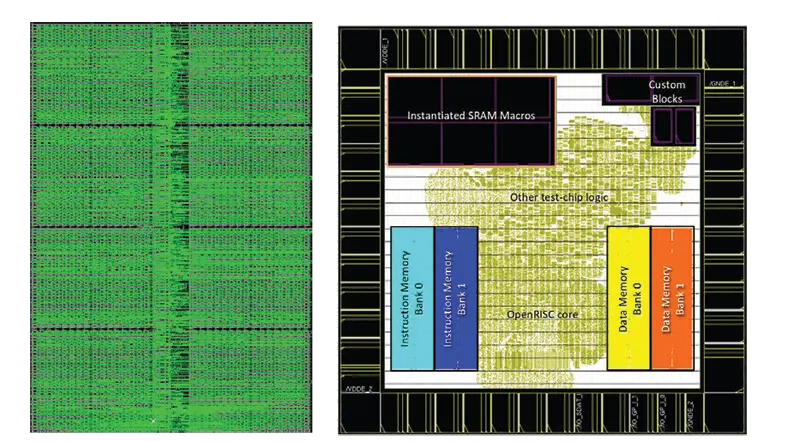
RAAAM™’s GCRAM technology has already been validated on silicon of leading semiconductor foundries in process nodes ranging from 16nm – 180nm and successfully evaluated in 5nm FinFET technology.

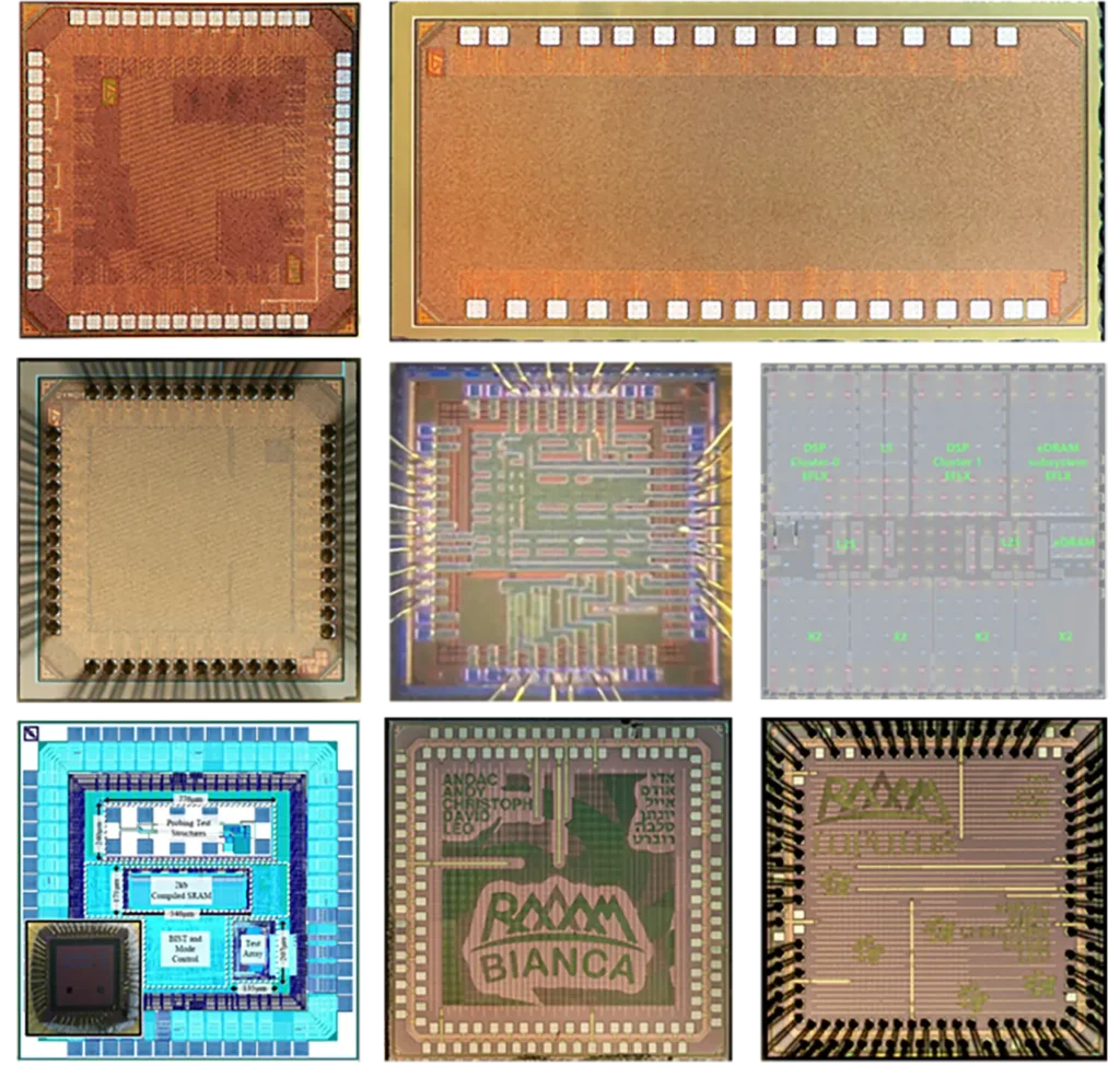
Microphotographs of Silicon Implementations of RAAAM™’s GCRAM Technology in 16nm-180nm Processes
SCM
RAAAM™’s Standard-Cell Memory (SCM) compiler offers a robust and fully automated solution to rapidly generate and efficiently integrate dozens of highly optimized local register files into SoCs and DSP accelerators. SCMs leverage the flexibility of any standard-cell library to compile small- and medium-size multi-ported memories of any arbitrary width and depth that integrate directly with your cell-based design flow without the overhead and limitations of SRAM register file IP macros. SCMs are compatible with any foundry CMOS process and require no IP qualification as they are 100% based on pre-qualified standard cells and also integrate directly with your cell-based floorplan without any area or design overhead. They are also compatible with aggressive voltage scaling to achieve ultra-low-power operation.
SCM Layout View after Guided Placement with 100% Density & Integration for 4 SCMs into an SoC
RAAAM™’s SCMs implement a highly optimized netlist that is tailored to your timing and area requirements and that are optimized for best-in-class power consumption. Automatically generated backend place & route guidelines lead to a nearly 100% density that introduces optimized area and power for read- and write access by up to 30% compared to RTL-based macros without guided placement.