Is RAAAM's embedded memory about to make a big difference?
By Peter Clarke
What’s at stake:
An Israeli-Swiss startup called RAAAM has gone back to the drawing board to design a CMOS-compatible memory that sits between SRAM and DRAM and that could offer a cost advantage for numerous applications, including artificial intelligence. If RAAAM can persuade a few foundries and fabless companies to adopt its approach, it could become an industry-changer.
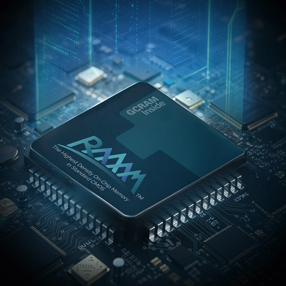
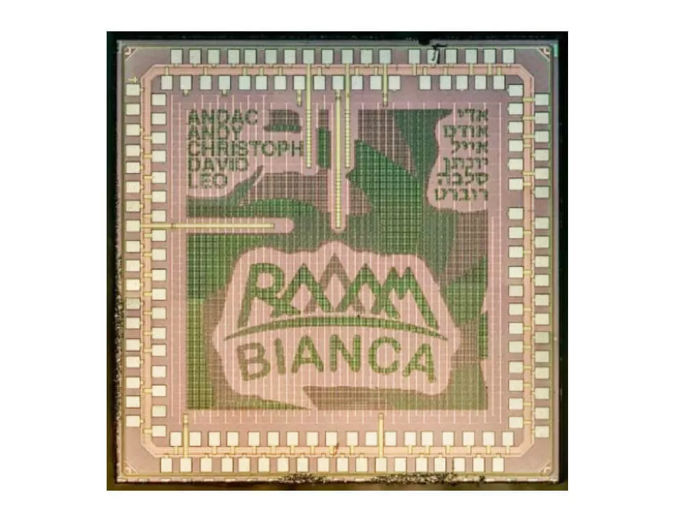
RAAAM Memory Technologies Ltd., headquartered in Pekah Tikva, Israel, and with an R&D base in Lausanne, Switzerland, is a 2021 startup that claims to have developed a better way to do embedded memory. The firm’s technology is called Gain-Cell RAM or GCRAM.
RAAAM claims it can achieve single-cycle SRAM read and write performance while providing up to a 50 percent area reduction and up to 10x power reduction compared with high-density SRAM. And GCRAM is fully compatible with standard CMOS fabrication flows, requiring no additional process steps.
RAAAM’s memory is dynamic rather than static, so it does require a periodic refresh cycle and associated peripheral circuitry. It has three transistors in its bit cell rather than DRAM’s one transistor, one capacitor. However, unlike DRAM, GCRAM can be easily integrated with CMOS logic.
SRAM typically has six transistors per bit cell, twice as many as the three-transistor GCRAM bit cell. So SRAM inherently takes up about twice the area of GCRAM and consumes about twice the power, all other things being equal. Additional peripheral circuitry to handle refresh cycles and make the GCRAM interface look like SRAM may reduce the advantage but for large memory arrays, such as 2Mbit, the density advantage should still deliver potentially major cost savings from the use of GCRAM instead of SRAM.
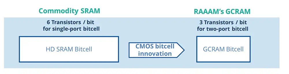
How RAAAM’s GCRAM differs from commodity SRAM (source: RAAAM)
The company’s plan is to be a memory IP licensor and it is working on macros that can be drop-in replacements for on-chip SRAM buffers and caches. Applications being targeted include AI weight input buffers, MCUs, automotive ADAS caches and image and video processing buffers.
Such technology-push developments from startups can be difficult to land if they run counter to industry practice and design-win convenience. But RAAAM already has a track record of shrinking its technology and asserts that SRAM is experiencing problems with scaling to next-generation process technologies.
Founders
The company was founded by CEO Robert Giterman, Andreas Burg, head of technology and an associate professor at Ecole Polytechnique Federal Lausanne (EPFL), and Professor Alex Fish of Bar-Ilan University, who serves as head of innovation. A fourth co-founder is Adam Teman, associate professor at Bar-Ilan University who serves as a scientific advisor.

Robert Giterman
“Bar-Ilan University and EPFL have been conducting collaborative research on the topic of on-chip memory for about a decade. There were research groups at each university developing technology that we are now commercializing,” Giterman told Ojo-Yoshida Report.
The research targeted volatile memory and the search for an alternative to SRAM. “The three-transistor DRAM was selected as the most promising. Giterman was heavily involved in the research having obtained his PhD at Bar-Ilan University and then moving to Switzerland to undertake post-doctoral research at EPFL.
RAAAM was set up in May 2021 and is making good progress, Giterman said. The company has signed an unnamed fabless chip company – one of foundry TSMC’s top ten customers – as a licensee and investor. RAAAM raised $4 million in a seed funding round and in July 2024 announced it had been awarded €5.25 million (about $5.8 million) from the European Innovation Council. This comprises a €2.5 million grant and a follow-on equity investment of €2.75 million.
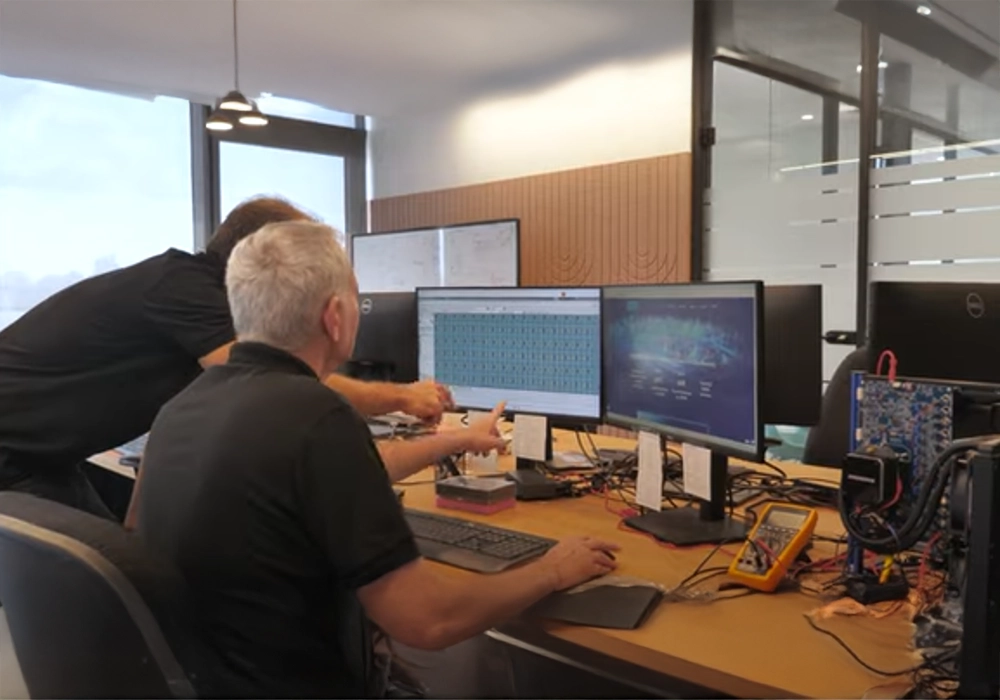
Having already designed test chips on a 16nm FinFET process, RAAAM is working with the unnamed licensee and TSMC on a test chip tape-out aiming for first 5nm GCRAM silicon in the first quarter of 2025. Giterman said that if the test chip performs as expected it could become a hard macro available for licensing. The company is also writing a compiler so that custom IP blocks can be generated.
SRAM problems, DRAM problems
One of the factors that Giterman says could drive the market towards GCRAM are the problems current memory systems are facing.
Most electronics applications are generating increasing amounts of data and requiring bigger and bigger memory spaces. Off-chip memory accesses, usually to DRAM, can be 1,000x more expensive in terms of latency and power than on-chip access.
As a result, larger on-chip SRAM caches are being adopted and in applications such as AI memory can be 70 percent of the area of an AI processor. RAAAM’s claims of 10x less power consumption partly derive from the ability to put larger, fast-access caches on the processor, reducing the rate at which data must be transferred from DRAM.
SRAM is already an area hog and in addition it has not been scaling as rapidly as logic, both in area and in operational voltage, Giterman observed. The latter is because an SRAM’s bit-line voltage and current drive needs to be elevated to overcome the bit-cell’s back-to-back inverters when writing. By way of contrast, Raaam has demonsrated a Vmin of 450mV for its GCRAM in a 16nm FinFET manufacturing process versus 700mV for standard on-chip SRAM. “The SRAM bit-cell structure means that if you scale aggressively you lose yield,” said Giterman.
The use of multiple transistors to make a dynamic RAM was already known before Bar-Ilan and EPFL started their research work. The topic had largely been ignored because of the success of the 1T1C DRAM. However, in an era of system-on-chip monolithic integration it has become relevant again. The academic research and RAAAM’s subsequent development work has focused on circuit design to reduce bit-cell leakage and thereby enhance data retention times. In addition, there are monitors and digital wrappers to run refresh algorithms that can be optimized for different applications.
Embedded DRAM
Corner case retention times of 10s of microseconds means that a refresh is required every 100 clock cycles or so at 1GHz clock frequency. Giterman said under these conditions 97 to 99 percent GCRAM availability is typically achievable. If an application has a predictable read/write pattern it is possible to ensure that refresh is happening when the application is unlikely to be trying to access the memory. This creates close to 100 percent availability.
Gain-Cell Embedded DRAMs for Low-Power VLSI Systems-on-Chip published by Springer in 2018
Conventional one-transistor embedded DRAM is, of course, denser than GCRAM but it has not been widely adopted in the semiconductor industry because of the trench capacitor needed for a 1T1C bit cell. This requires additional mask layers beyond what is on offer in CMOS logic processes and has more or less killed off eDRAM as an option.
The complexity around the basic multi-transistor DRAM is what RAAAM has been covering with patents and will protect the company from competitors, Giterman reckons. But what is needed to make GCRAM a success?
“GCRAM needs to go through the full qualification process, be accepted by foundries and the rest of the IP ecosystem,” said Giterman. “We plan to go through this at 5nm over the next 18 months. We achieved proof of concept at 16nm and as part of the academic research we made GCRAM on FDSOI and bulk 28nm CMOS,” he said.
RAAAM has achieved all this with remarkably little funding but it is now in the process of closing a Series A round. “We already have commitments from a number of investors. We are planning to close the round by the end of the year at about $15 million,” he said.
Bottom line:
With the inconvenience of dynamic refresh abstracted away then a three-transistor embedded DRAM that is CMOS compatible could become a drop-in replacement for SRAM. If it can offer the same performance as SRAM with lower power consumption and a smaller die area it could be a disruptor in the memory market. More than one high profile adopter and the support of TSMC are likely to be enablers of success.
Peter Clarke is a veteran reporter and analyst covering the global electronics industry.
This article was first published by The Ojo-Yoshida Report on September 17, 2024. See www.ojoyoshidareport.com for more of such reports.